

NVIDIA A40 vs A100: Full Benchmark Comparison for AI, Rendering, and Video Editing
Compare the NVIDIA A40 and A100 to discover which GPU offers the best balance of performance, features, and value for AI workloads, 3D rendering, video editing, and professional compute tasks.
NVIDIA A40 vs A100 – Background Comparison
| Brand | Series | Model | Release Year | Official Positioning | Market Price (USD) |
|---|---|---|---|---|---|
| NVIDIA | Data Center (Ampere) | A40 | 2020 | Built on NVIDIA’s Ampere architecture, the A40 is designed for data-center graphics, visualization, and VDI workloads. With 48GB GDDR6 memory, strong CUDA performance, and support for ray tracing and AI acceleration, it is well-suited for remote workstations, rendering, CAD, digital content creation, and mixed compute workloads. | ~$5,500 – $1,0000 + |
| NVIDIA | Data Center (Ampere) | A100 | 2020 | The A100 is NVIDIA’s flagship AI and HPC accelerator, built on the Ampere architecture. Featuring Tensor Cores, massive parallel compute capability, and up to 40GB / 80GB HBM2e memory, it delivers industry-leading performance for AI training, inference, scientific computing, and large-scale data analytics. | ~$8,000 – $14,000+ |
NVIDIA A40 vs A100– Specifications Comparison
Core Specs Comparison between NVIDIA A40 vs A100
| Specification | A100 | A40 | A100 Improvement / Gain |
|---|---|---|---|
| GPU Model | NVIDIA A100 | NVIDIA A40 | — |
| Architecture | Ampere | Ampere | — |
| CUDA Cores | 6,912 | 10,752 | A40 has ~55% more CUDA cores |
| Memory Type | HBM2e | GDDR6 | HBM2e offers much higher bandwidth & lower latency |
| Memory Capacity | 40GB / 80GB | 48GB | Up to +67% (80GB vs 48GB) |
| Memory Bandwidth | ~1,555 GB/s | ~696 GB/s | ≈2.2× higher bandwidth |
| Core Frequency (Base / Boost) | ~765 / 1,410 MHz | ~1,305 / 1,740 MHz | A40 has higher clock speeds |
| TDP (Power Draw) | 250W (PCIe) / 400W (SXM) | 300W | Better performance per watt for AI/HPC |
| Interface | PCIe / SXM4 | PCIe | SXM enables higher scalability |
| FP32 Performance | ~19.5 TFLOPS | ~37.4 TFLOPS | A40 stronger in raw FP32 |
| Tensor Cores | 432 (3rd Gen) | 336 (3rd Gen) | ~29% more Tensor Cores |
| PCIe Interface | PCIe 4.0 x16 | PCIe 4.0 x16 | — |
Summary:The NVIDIA A100 and A40 are both built on the Ampere architecture, but they target very different use cases. The A100 is designed primarily for AI training, inference, and high-performance computing, leveraging HBM2e memory with more than twice the memory bandwidth of the A40 and a higher number of third-generation Tensor Cores, which results in significantly better performance for large-scale AI and data-intensive workloads. By contrast, the A40 focuses on graphics, visualization, and virtual workstation scenarios, offering higher core clock speeds and stronger raw FP32 performance that benefit rendering, CAD, and VDI applications. In essence, the A100 is optimized for compute-heavy AI and HPC tasks, while the A40 is better suited for graphics-centric and mixed workloads.
Advanced Feature Comparison between NVIDIA A40 vs A100
| A100 | A40 | A100 Improvement / Gain |
|---|---|---|
| Supports Multi-Instance GPU (MIG) up to 7 isolated instances | Not supported | Enables secure GPU partitioning and concurrent workloads |
| NVLink support via SXM4 (up to 600 GB/s interconnect) | No NVLink support | Allows far superior multi-GPU scaling |
| FP16 / BF16 Tensor performance up to 312 TFLOPS | ~149 TFLOPS FP16 | ≈2.1× faster AI compute throughput |
| INT8 / INT4 Tensor acceleration | INT8 only | Higher inference performance and lower latency |
| Optimized for training large language models (LLMs) and massive datasets | Limited support for large models | Better performance on large-scale AI tasks |
| High-performance computing (HPC) ready, e.g., LINPACK, CFD | Not HPC-focused | Significant advantage in scientific computing |
| AI performance per watt optimized | Graphics-focused efficiency | More energy-efficient for AI workloads |
| Designed for GPU clusters & supercomputers | Targeted at VDI and visualization | Enterprise-scale AI deployment advantage |
| Ultra-low memory access latency (HBM2e) | Higher memory latency (GDDR6) | Faster data feeding to compute units |
| Future AI framework compatibility (FP16, BF16, Tensor ops) | Limited AI acceleration | Better long-term value for AI applications |
Summary:The NVIDIA A100 outshines the A40 in advanced compute workloads, leveraging MIG support for isolated GPU instances, NVLink for high-speed multi-GPU scaling, HBM2e ultra-high bandwidth memory, and superior FP16/BF16 and INT8/INT4 Tensor Core performance. These features enable the A100 to excel in large-scale AI training, inference, and HPC applications, delivering significantly higher throughput, lower latency, and better energy efficiency. In contrast, the A40 is optimized for graphics, visualization, and virtual workstation tasks, making the A100 the clear choice for compute-intensive, data-heavy environments.
NVIDIA A40 vs A100 Performance Across Different Scenarios
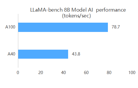
Artificial Intelligence Testing
Based on the benchmark results, the A100 delivers approximately 1.8–1.9× higher inference throughput than the A40 for the LLaMA‑8B model. This advantage stems from its greater number of Tensor Cores, superior FP16/BF16 performance, high-bandwidth HBM2e memory, and support for NVLink and MIG. In contrast, the A40’s fewer Tensor Cores, lower memory bandwidth, and lack of NVLink/MIG support constrain its performance on large-scale AI workloads.
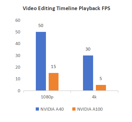
Editing Performance
The benchmarks show the A40 significantly outperforms the A100 in video editing. At 1080p, the A40 achieves 50–60 FPS vs 15–25 FPS for the A100; at 4K, 30–40 FPS vs 5–10 FPS. This is because the A40 is optimized for graphics and video workloads with higher FP32 performance, more CUDA cores, and hardware video acceleration, while the A100 is designed for AI/HPC and lacks video pipeline optimizations.
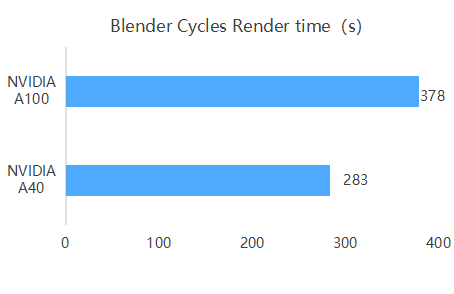
3D Rendering
The Blender Cycles benchmark shows the A40 renders ~33% faster than the A100 (283 s vs 378 s). This is because the A40’s more CUDA cores and higher frequencies favor traditional rendering, while the A100 is optimized for AI/HPC workloads, making it less efficient for standard GPU rendering.
Price & Value: NVIDIA A40 vs A100
The NVIDIA A40 and A100 target different workloads, with the A100 typically costing 2–3× more than the A40. The A100 excels in AI, HPC, and large-scale compute thanks to MIG, NVLink, HBM2e memory, and advanced Tensor Cores, while the A40 is optimized for graphics, visualization, and VDI. For graphics-focused tasks, the A40 is more cost-efficient, whereas the A100 is the clear choice for compute-intensive, data-heavy workloads.
Price Comparison
| Platform / Retailer | NVIDIA A40 (USD) | NVIDIA A100 (USD) | Price Difference (USD) | Price Difference (%) |
|---|---|---|---|---|
| Official MSRP | ~$5,500 | ~$15,000 | –$9,500 | –63% |
| Retail / Resellers | ~$5,000–$8,000 | ~$10,000–$23,000 | –$5,000–$15,000 | –50%–65% |
| Secondary / Marketplace | ~$4,500–$7,500 | ~$9,000–$20,000 | –$4,500–$12,500 | –50%–62% |
User Value-for-Money Feedback
User value-for-money feedback generally shows that the NVIDIA A40 delivers strong performance per dollar for graphics, visualization, and VDI workloads compared with the A100, because it costs significantly less while still handling most rendering and mixed compute tasks effectively. The A100, although much more expensive, provides MIG support, NVLink connectivity, HBM2e memory, and superior Tensor Core performance, making it the better value only if AI training, inference, or large-scale HPC workloads are the priority.
NVIDIA A40 vs A100 – Pros & Cons
| Model | Pros | Cons |
|---|---|---|
| NVIDIA A40 | ✅ Strong performance for graphics, visualization, and VDI workloads ✅ Excellent price-to-performance for rendering and mixed compute tasks ✅ Lower cost than A100 ✅ Efficient for most 3D, CAD, and visualization workloads |
❌ Lacks advanced AI/HPC features like MIG, NVLink, and HBM2e memory ❌ Limited for large-scale AI training and inference ❌ Not ideal for multi-GPU HPC clusters |
| NVIDIA A100 | ✅ Exceptional AI and HPC performance with Tensor Cores ✅ Supports MIG for GPU partitioning and NVLink for multi-GPU scalability ✅ Ultra-high bandwidth HBM2e memory ✅ Optimized for large-scale AI models, HPC, and data-intensive workloads |
❌ Significantly higher cost than A40 ❌ Overkill for graphics-focused or VDI tasks ❌ Requires specialized infrastructure for full utilization |
NVIDIA A40 vs A100 Hosting
The NVIDIA A40 and A100 cater to different performance needs in the data-center and AI/HPC space.
For organizations or teams that require flexible GPU resources without heavily investing in local hardware, GPU hosting provides a scalable and cost-effective solution. Database Mart offers A40 GPU servers and A100 GPU servers , giving access to powerful compute resources.
The A40 efficiently handles graphics-centric workloads and is well-suited for graphics, visualization, rendering, and virtual workstation tasks, delivering cost-effective performance for 3D modeling, CAD, and other GPU-accelerated applications.
The A100, on the other hand, provides exceptional AI training, inference, and HPC performance with features such as MIG, NVLink, HBM2e memory, and advanced Tensor Cores, making it the ideal choice for large-scale AI models, HPC workloads, and data-intensive projects.
Conclusion
NVIDIA A40: High-end data-center GPU optimized for graphics, visualization, rendering, and virtual workstation workloads. Cost-efficient for 3D modeling, CAD, and GPU-accelerated tasks. Not ideal for large-scale AI or HPC workloads due to memory and compute limitations.
NVIDIA A100: Flagship data-center GPU designed for AI training, inference, and high-performance computing. Features MIG, NVLink, HBM2e memory, and advanced Tensor Cores, enabling large-scale AI models and HPC workloads. Higher cost and specialized infrastructure required.
Summary: The A40 delivers strong performance for graphics-focused tasks at a lower cost, while the A100 dominates compute-intensive AI and HPC workloads, making it the preferred choice for large-scale, data-heavy applications.
A40 vs A100, a40 vs a100 performance, nvidia a40 vs a100 benchmark, nvidia a40 vs a100 price, a40 vs a100 speed, a40 vs a100 gpu, nvidia ampere a40 vs a100